Flik-o-meter build guide
The flik-o-meter is a small hand-held light sensor that you hold against a monitor to measure what the screen actually shows. A photodiode with a built-in amplifier (the TI OPT101) turns the light from one flickering target into a voltage; an Arduino Nano samples that voltage 2000 times a second and streams the raw samples over USB; the toolbox on the PC works out the flicker frequency and how steady it is, and checks it against the frequency the experiment's design asked for. It measures flicker from about 8 Hz to 100 Hz, hard on/off or smoothly modulated, to within ±0.1 Hz. It is a frequency and timing instrument, not a light meter: it does not report luminance in cd/m².
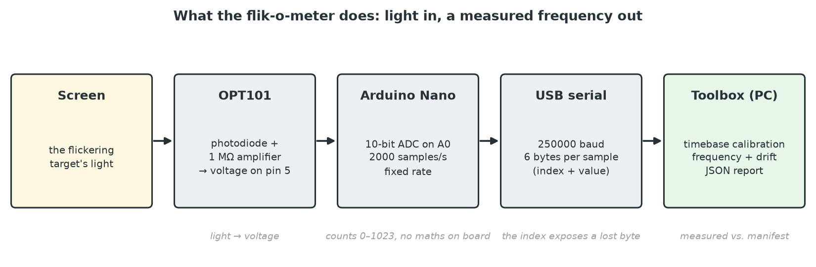
Figure 1. What each part does. The board only samples and sends; every calculation happens on the PC.
You build it in two stages. Stage 1 wires the circuit on a solderless breadboard so you can prove the parts and the firmware work before you solder anything. Stage 2 builds the finished wand: the sensor on a small board in the nose of a 3D-printed case, the Arduino behind it, and a strain-relieved USB cable out the back.
Bill of materials
Prices are approximate, in US dollars, for single units. Part numbers are examples; any equivalent part works unless the notes say otherwise.
Electronics (per unit)
| Ref | Part | Value / spec | Qty | Purpose | Example part numbers | Approx. cost |
|---|---|---|---|---|---|---|
| U1 | Light sensor | TI OPT101P: photodiode and transimpedance amplifier in one 8-pin DIP | 1 | Turns light into a voltage the Arduino can read directly | TI OPT101P (Digi-Key 296-23090-5-ND, also Mouser) |
$10–15 |
| — | Microcontroller board | Arduino Nano, ATmega328P, 5 V, 16 MHz | 1 | Samples the sensor at a fixed rate and streams the samples over USB | Arduino A000005 (Digi-Key 1050-1006-ND) |
$25 |
| — | IC socket | 8-pin DIP, 0.3 in row spacing | 1 | Holds the OPT101 so it can be removed or replaced without desoldering | Adam Tech ICS-308-T; machined-pin upgrade ICM-308-1-GT |
$0.20–0.60 |
| C1 | Decoupling capacitor | 0.1 µF ceramic, ≥ 16 V, through-hole (often marked "104") | 1 | Steadies the OPT101's supply | KEMET C320C104K5R5TA7317, or any 0.1 µF X7R |
< $1 |
| SW1 | Start button (optional) | 6 mm tactile momentary switch | 1 | Starts each measurement from the wand, so you don't have to reach for the keyboard | Omron B3F-1000 (Digi-Key SW262-ND) |
$0.10–0.50 |
| — | Perfboard | 0.1 in pitch FR-4; you need one piece no bigger than 20 × 15 mm | 1 | Carries the socket and C1 in the nose of the wand | Adafruit 4783 (2 × 8 cm, pack of 3), cut down |
$5 per pack |
| — | Hookup wire | 22–26 AWG; stranded for the leads inside the wand, in red, black and yellow if you can | ~ 30 cm | Connections between the nose board and the Nano | any | ~ $0 |
| — | USB cable | Mini-B to your PC's port; must carry data, not only charge | 1 | Power and data | any | $2–5 |
Enclosure and mechanical (per unit)
| Part | Value / spec | Qty | Purpose | Source | Approx. cost |
|---|---|---|---|---|---|
| Wand case | 3D-printed PETG, two halves, black or another opaque dark colour | 1 set | Holds everything; the nose is the light shield | flikometer_nano_bottom.stl and flikometer_nano_top.stl in this folder (source: flikometer_enclosure.scad) |
~ $1 of filament |
| Contact ring | TPU print, a silicone O-ring of about 15 mm outside diameter, or adhesive foam | 1 | Soft tip that rests on the screen without scratching it; glue it to the tip face for now (#554) | — | ~ $0 |
| Screws and inserts | 2 × M2 screws and 2 × M2 brass heat-set inserts (or 2 self-tapping screws) | 2 sets | Closes the case so it can be opened again | — | ~ $0.50 |
| Zip tie | small | 1 | Strain relief for the USB cable | — | ~ $0.05 |
| Mounting tape or hot glue | double-sided foam tape | small | Holds the Nano and the nose board in place | — | ~ $0 |
A complete unit costs roughly $40–45; the Nano and the OPT101 are most of it.
For Stage 1 only (reusable)
| Part | Value / spec | Qty | Approx. cost |
|---|---|---|---|
| Solderless breadboard | half-size (30 columns) or larger, with power rails | 1 | $5 |
| Jumper wires | solid-core 22 AWG, or a pre-cut jumper kit (stranded wire does not seat in breadboard contacts) | ~ 12 | $5 |
| Black card or heat-shrink | to roll a short tube around the sensor | — | ~ $0 |
Alternatives
- Other Arduino boards. The firmware runs on any 5 V ATmega328P board (Uno R3, Adafruit Metro Mini 328, Nano clones). The genuine Nano is recommended because three things were made for it: the firmware has been verified on it, the printed case is sized for it, and the toolbox's Measure flicker dialog recognises its USB chip (an FTDI FT232R) and selects its port for you. With another board you pick the port by hand, may need a USB driver (most clones use a CH340 chip), may need the "old bootloader" upload setting, and must re-measure the case before printing. An Uno does not fit the case at all.
- No OPT101? A Vishay BPW34 photodiode feeding an MCP6002 op-amp wired as a transimpedance amplifier (feedback resistor 100 kΩ–1 MΩ with a 15–22 pF capacitor across it) does the same job with more parts. Use a rail-to-rail op-amp like the MCP6002, not an LM358, whose output cannot swing close to 0 V. Do not connect a bare photodiode and a large load resistor straight to the Arduino's input; see Design notes.
- Measuring contrast or luminance. See A photometric variant.
Tools
- Temperature-controlled soldering iron with a fine tip, and rosin-core solder
- Flush cutters, wire strippers, small pliers or tweezers
- Multimeter with continuity (beep) and DC volts
- A craft knife or scoring tool to cut the perfboard
- A 3D printer that prints PETG (and TPU, for the ring), or a printing service
- A heat-set insert tip for the iron, or the iron's ordinary tip used gently
- A PC with a USB port and the toolbox installed
Safety
- Flicker. Testing shows flickering targets on the screen. Flicker can trigger seizures in people with photosensitive epilepsy; anyone with that history should not run or watch the tests. Esc in the stimulus window, or Abort in the dialog, stops a test at any time.
- Soldering. The iron and freshly melted heat-set inserts are hot enough to burn. Work with ventilation and keep solder fumes away from your face. If your solder contains lead, wash your hands afterwards and don't eat at the bench.
- Cutting perfboard. Score and snap it; don't saw or sand FR-4 dry, because the glass-fibre dust irritates skin and lungs.
- Electrical. Everything runs from the USB port's 5 V and is low risk, but a short between 5 V and ground can make the PC shut the port down. Unplug USB before changing any wiring.
- The screen. Rest the tip on the glass; don't press. LCD panels can be marked permanently by pressure.
How the circuit works
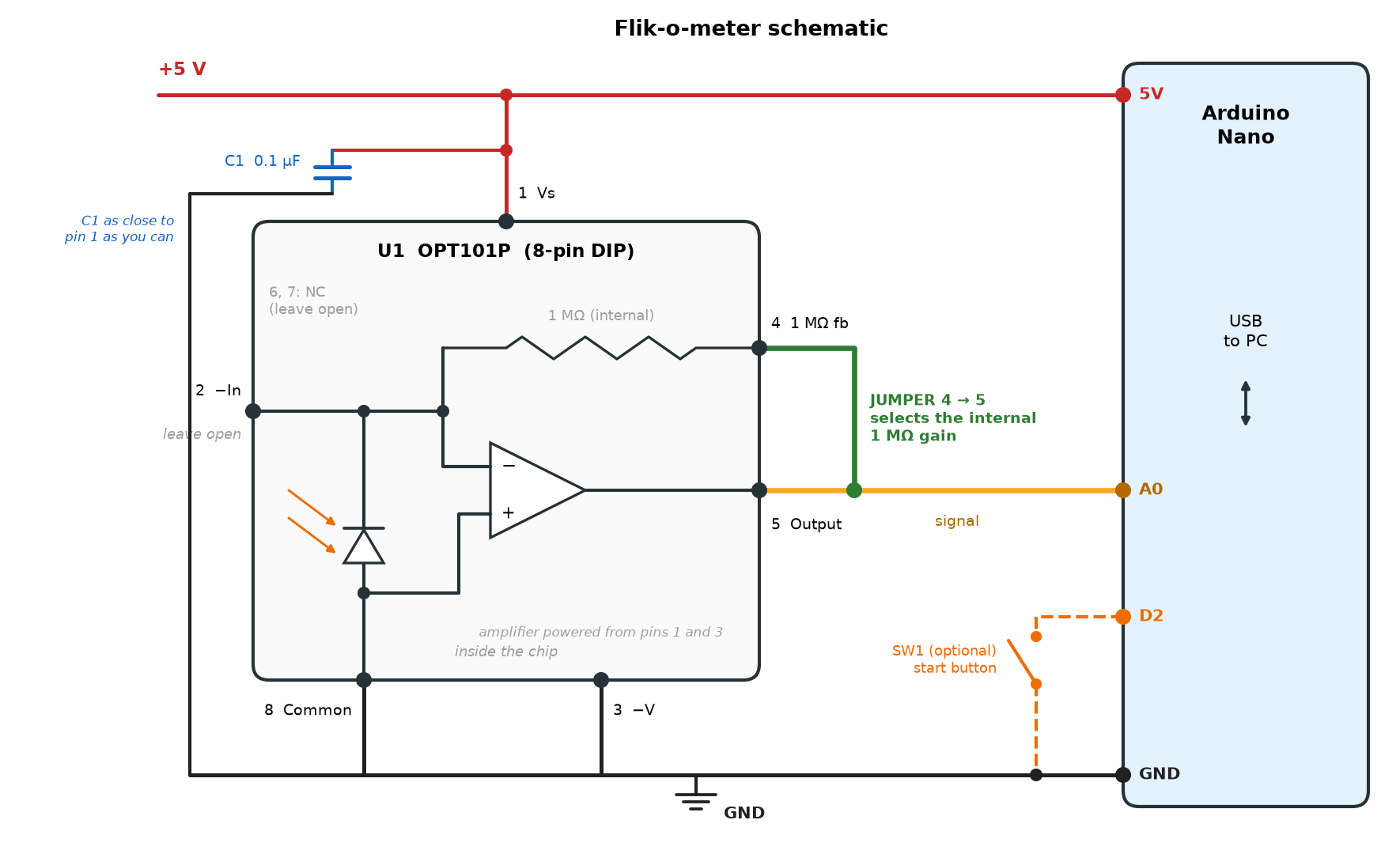
Figure 2. The whole circuit. The rounded box is the OPT101; you only make the connections outside it.
The OPT101 contains a photodiode and an amplifier that converts the photodiode's tiny current into a voltage. Joining pin 4 to pin 5 puts the chip's internal 1 MΩ resistor in the amplifier's feedback path, which sets the gain: about 0.45 V per microwatt of light at 650 nm. Pin 5 then carries a voltage that follows the light, and it goes straight to the Arduino's analogue input A0. The Arduino's 10-bit converter reads 0–5 V as 0–1023 counts, about 4.9 mV per count.
| OPT101 pin | Name | Connect to | Why |
|---|---|---|---|
| 1 | Vs (supply) | Arduino 5V | Power. C1 goes from this pin to ground, as close to the pin as you can. |
| 2 | −In | nothing | Only used for an external gain resistor (Gain and other adjustments). |
| 3 | −V | GND | Negative supply, which is ground here. |
| 4 | 1 MΩ feedback | pin 5 | The jumper that selects the internal 1 MΩ gain. The connection most often forgotten. |
| 5 | Output | Arduino A0 (and pin 4) | The light signal. |
| 6, 7 | not connected | nothing | |
| 8 | Common | GND | The photodiode's other side. |
Pin 1 is at the end of the chip marked with a notch or dot. Looking at the chip from above with the notch on the left, pins 1–4 run left to right along the bottom edge and pins 5–8 run right to left along the top, so pin 4 sits directly opposite pin 5.
The optional start button connects Arduino pin D2 to GND. The firmware turns on D2's internal pull-up resistor, so no other part is needed, and a board without a button works the same.
Software and firmware
You need the toolbox installed on the PC (see its installation instructions), and a way to upload firmware to the Arduino. The steps below use arduino-cli, which needs no Arduino IDE; the IDE works too (board Arduino Nano, processor ATmega328P).
Install arduino-cli (once)
On Windows:
winget install --id ArduinoSA.CLI --exact --silent --accept-package-agreements --accept-source-agreements
& "C:\Program Files\Arduino CLI\arduino-cli.exe" core update-index
& "C:\Program Files\Arduino CLI\arduino-cli.exe" core install arduino:avr
arduino-cli installs to C:\Program Files\Arduino CLI and is not added to PATH. Either call it by its full path, as above, or add it for the session with $env:Path = "C:\Program Files\Arduino CLI;$env:Path". On macOS use brew install arduino-cli; on Linux, the download from https://arduino.github.io/arduino-cli/. Then run the same two core commands.
Find the board's port
Plug the board in and run:
The port that appears when you plug the board in is the one you want (on Windows, COM and a number; on macOS, /dev/tty.usbserial-… or /dev/tty.usbmodem…). A genuine Nano shows as an Unknown board with USB ID 0403:6001. That is expected: its FTDI USB chip carries no Arduino identifier, so you name the board yourself in the commands below.
Upload a sketch
Two sketches live in firmware/ (paths below are relative to this folder, hardware/flikometer/):
firmware/bringup/prints readings as text. You use it once, in Stage 1, to check the sensor.firmware/flikometer/is the real firmware. It streams binary data for the toolbox and is what the finished device runs.
arduino-cli compile --fqbn arduino:avr:nano firmware/flikometer
arduino-cli upload  -p COM5 --fqbn arduino:avr:nano firmware/flikometer
Replace COM5 with your port, and firmware/flikometer with firmware/bringup for the check sketch. The streaming firmware compiles to about 2.3 kB (7 % of the Nano's memory).
If the upload fails with a sync error (avrdude: stk500_recv() or not in sync), the board has the old bootloader, as Nanos made before about 2018 and most clones do. Upload again with:
That error does not mean the board is damaged. For other boards use --fqbn arduino:avr:uno (Uno R3 and Adafruit Metro Mini 328).
Stage 1: breadboard prototype (no soldering)
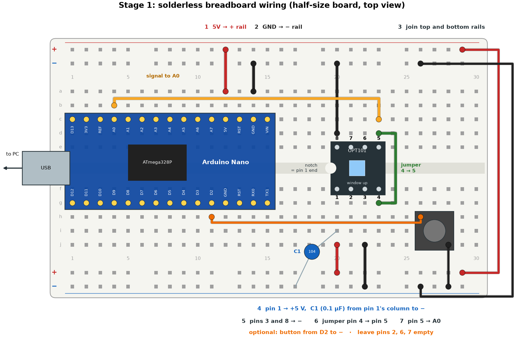
Figure 3. One working layout on a half-size breadboard. Column numbers and row letters are only a guide; what matters is which pins share a column.
On a breadboard, the five holes in each half-column (a–e, or f–j) are connected to each other, and the long rails along the edges carry power. The OPT101 and the Nano each straddle the centre channel so that every pin gets its own column.
- Unplug USB. Do all wiring with the board unpowered.
- Seat the Nano across the centre channel at the left end, USB connector pointing outward.
- Power rails. Wire the Nano's 5V pin to the + rail and its GND pin to the − rail. If the breadboard has rails at the top and bottom, join top + to bottom + and top − to bottom −.
- Checkpoint: no short. With the multimeter on continuity, touch the + rail and the − rail. It must not beep.
- Seat the OPT101 across the centre channel to the right of the Nano, notch toward the Nano, clear window facing up. Confirm where pin 1 is before going on (Figure 3 shows the pin numbers).
- Pin 1 to +5 V. Wire pin 1's column to the + rail. Fit C1 from pin 1's column to the − rail, with short leads and the body close to the chip.
- Pins 3 and 8 to ground. Wire each to the − rail.
- The feedback jumper. Wire pin 4 to pin 5. They are in the same column on opposite sides of the channel, so this is a short wire across the chip.
- Pin 5 to A0. Wire pin 5's column to the Nano's A0 pin.
- Leave pins 2, 6 and 7 empty.
- Optional button. Fit the button across two free columns; wire one side to the Nano's D2 and the other to the − rail.
- Checkpoint: wiring. Still unpowered, check with the meter's continuity setting:
- OPT101 pins 3 and 8, C1's ground leg and the Nano's GND all beep to each other;
- pin 1 beeps to the Nano's 5V; pin 5 beeps to A0 and to pin 4;
- 5V does not beep to GND.
- Power up. Plug in USB. The Nano's power LED lights. If it doesn't, or the PC warns about a USB power surge, unplug at once and look for a short.
- Checkpoint: voltages. With the meter on DC volts, black probe on GND: OPT101 pin 1 reads about 4.5–5.0 V. Pin 5 reads close to 0 V with the window covered by something opaque (a coin or black tape; not a fingertip, which passes red and infrared light) and rises in room light.
- Upload the check sketch (
firmware/bringup; see Upload a sketch) and open a serial monitor at 9600 baud:arduino-cli monitor -p COM5 -c baudrate=9600, or the IDE's Serial Plotter. Readings scroll about 50 times a second. -
Checkpoint: the sensor responds. Compare what you see with this table. The check sketch reads too slowly to see flicker; it only proves that the sensor follows light.
You see Meaning What to do A few hundred counts in room light; near 0 when covered; higher toward a lamp Working Go on to step 17 Stuck at 0, or no response to light Wiring fault Check, in this order: the pin 4 → pin 5 jumper, which way round the chip is, the ground wires on pins 3 and 8 Stuck at 1023 A0 is wired to 5 V, not to pin 5 Recheck step 9 Flat at the same high value however bright the light The sensor is saturated (it cannot drive its output all the way to 5 V, so this flat top sits below 1023) Normal under a bright lamp; on a screen, see Gain and other adjustments A swing of less than about 100 counts between covered and room light Weak signal Move closer to the light; the internal 1 MΩ is already near the most useful gain Jumpy, noisy numbers Ground or decoupling Move C1 closer to pin 1; make sure pins 3 and 8 go to the same ground -
Upload the streaming firmware (
firmware/flikometer). The serial monitor now shows unreadable characters, which is correct: the data are binary. Close the monitor, because only one program can hold the port. - Make a sensor snout. Roll a short tube of black card or heat-shrink, about 6 mm across and tall enough to stand above the Nano, and slip it over the OPT101. It lets you hold the breadboard against the screen and limits what the sensor sees to one spot. Don't seal it light-tight against the screen: a little room light must get in (see Troubleshooting, "every target fails as clipped at 0").
-
Functional test with the toolbox. Start a measurement with the full-contrast sync square, which gives you one fixed spot to hold the sensor on:
Or in the toolbox: open a design in Design mode, click Measure flicker…, pick the port (a genuine Nano is found and selected for you), tick Sync square, and click Start.
For the first minute the toolbox measures the board's true sample rate, and no window appears; leave the sensor anywhere. Then the stimulus window opens. Hold the snout on the flashing square in the bottom-left corner and press SPACE for each target; keep it there for the whole run.
-
Checkpoint: expected readings. A healthy prototype prints something like this (the target names and numbers will differ):
timebase: declared 2000 Hz → measured 2000.79 Hz (+0.040 %) T1: nominal 40 Hz | measured 40.012 Hz | Δ +0.012 Hz | drift 0.12 ms | adc 6-222 | PASS ... 9/9 targets passed; report → qc-reports/flikometer_<design>_<fingerprint>_<time>.json- The measured sample rate is within ±0.5 % of 2000 Hz (1990–2010 Hz).
- Each target PASSes, with Δ within ±0.1 Hz.
- The
adcrange stays clear of both 0 and 1023. - No line mentions
desync.
If that is what you see, the circuit and the firmware are proven and you can build the final version. If not, see Troubleshooting.
Stage 2: final build
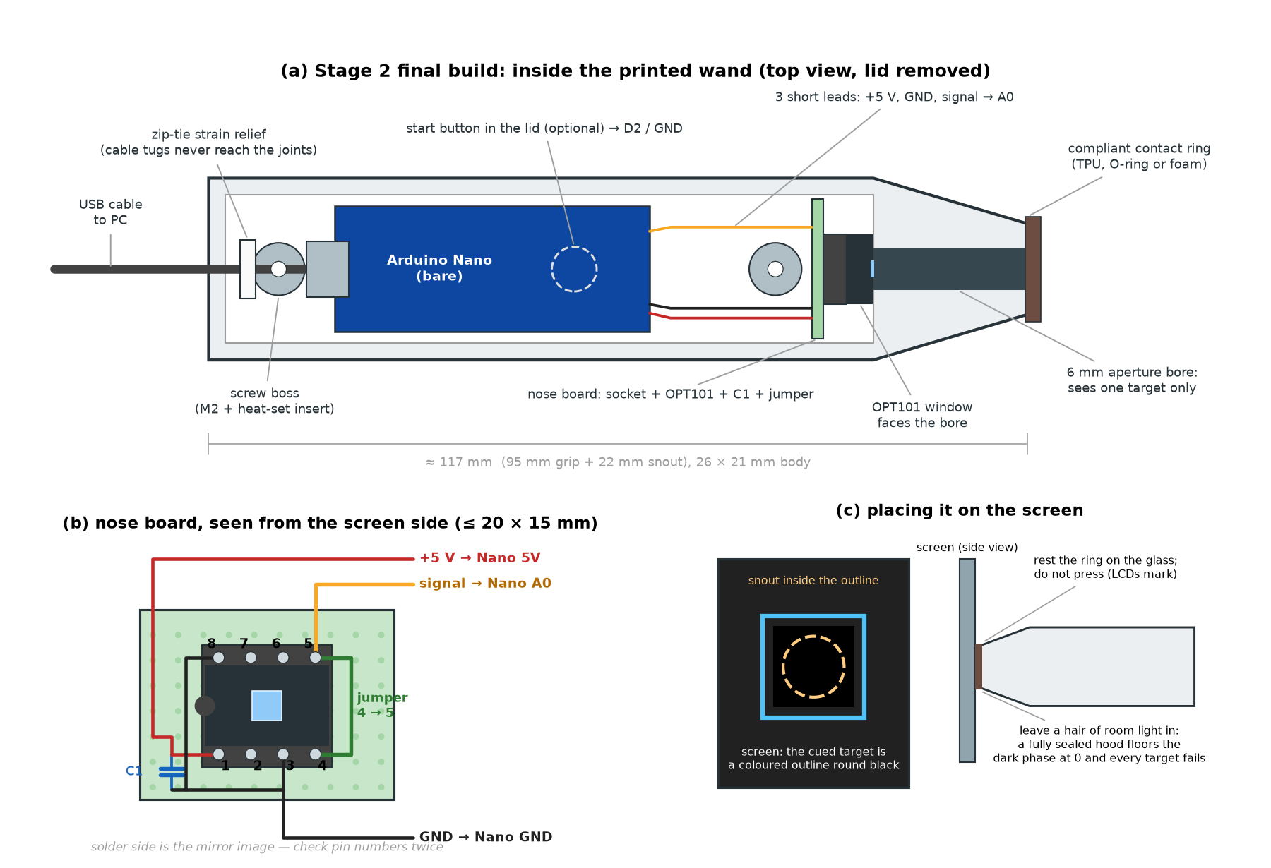
Figure 4. (a) The finished wand with the lid removed, drawn to the case's default dimensions. (b) The nose board seen from the screen side. (c) How it sits on the screen.
In the finished wand the Nano sits bare in the body, USB toward the back. The OPT101 stands on a small board in the nose, looking forward down a 6 mm bore that lets it see only one target. Three short leads join them. Only the USB cable leaves the case.
Print the case
- Print a fit test first. Crop the STL in your slicer to the nose and a short stub of the body (cut at about z 70 mm; the
.scadhas no separate fit-test part yet, see #554), print that, and check the nose board, the bore and the Nano against your actual parts. Boards vary. If anything is tight, changebody_w,body_h,grip_lenandwallinflikometer_enclosure.scad: those are the parameters that size the board bay.board_l,board_w,comp_h,pcb_tandcable_din the same block are currently unused, so changing them does nothing (#554). If your Nano came with header pins fitted, check they clear the bay too. - Print both halves in PETG, in black or another opaque dark colour: a pale or thin shell lets room light through to the sensor. Use 0.2 mm layers and at least 3 perimeters, each half lying flat on its parting face; no supports are needed. The ready-made
flikometer_nano_bottom.stlandflikometer_nano_top.stlare for the genuine Nano. To make your own, open the.scadin OpenSCAD (free), setpart = "bottom", render (F6) and export STL, then repeat withpart = "top"; or, without the GUI,openscad -o bottom.stl -D 'part="bottom"' flikometer_enclosure.scad. - Make the contact ring. Print a plain ring in TPU about 15 mm across, or use a silicone O-ring or a ring of adhesive foam. Glue it to the tip face. The current case has no recess for it to press-fit into (the recess is wider than the 13 mm tip, #554), so do not rely on a fit.
Build the nose board
- Cut the perfboard to no more than 20 × 15 mm by scoring both sides along a row of holes and snapping it, then clip or file the corners (the case's bay has rounded corners of about 2.6 mm radius). The board stands upright inside the nose, so it must fit the case's inner cross-section (about 21 × 16 mm).
- Solder the socket, empty, in the middle of the board, so the OPT101's window will face the bore. Mark the pin-1 end on the board.
- Solder C1 from the socket's pin 1 to a free pad beside it that will be the ground point, with the leads as short as you can.
- Make the links on the solder side: pin 4 to pin 5; pin 3 and pin 8 to C1's ground pad. Leave 2, 6 and 7 unconnected.
- Attach three stranded leads, each about 6–8 cm long (long enough to reach the Nano with a little slack): red from pin 1, black from the ground pad, yellow from pin 5. Figure 4b shows the board from the component side; the solder side is its mirror image, so check every pin number twice.
- Checkpoint: inspect before the chip goes in. With the socket still empty, look for solder bridges between neighbouring pins, then check each connection in the pin table with the meter. Red must not beep to black.
Wire the Nano
- Solder the leads to the Nano's pads: red to 5V, black to GND, yellow to A0.
- Optional button. Solder two leads, about 6 cm long, from the Nano's D2 and its other GND pin to the two sides of the tactile button. The button sits in the hole in the lid.
- Seat the OPT101 in its socket, pin 1 to the marked end.
- Checkpoint: test before closing. Plug in USB and repeat steps 19–20 of Stage 1 with the parts loose on the bench. A circuit that worked on the breadboard and fails now almost always has a bad joint: reflow the suspect joints before rewiring anything.
Assemble
- Heat-set inserts. Press the two M2 inserts into the bosses of the bottom half with the iron. (Set
use_heatset = falsein the.scadto print holes for self-tapping screws instead.) - Mount the nose board upright directly behind the bore, the OPT101's window centred on it and square to it, held with foam tape or a dab of hot glue. Centring matters: the bore is what stops the sensor seeing neighbouring targets.
- Mount the Nano in the bay between the two bosses, USB toward the back opening, with foam tape or hot glue.
- Strain relief. Plug in the USB cable, route it out of the back hole, and zip-tie it to itself just inside the back wall, so a pull on the cable is taken by the tie and the case, never by the solder joints. Cable tugs are the commonest way a hand-held USB device fails.
- Close the case. Fit the button through its hole, seat the alignment pins, and screw the top half into the inserts.
- Glue the contact ring to the tip face, centred on the bore (the case has no usable recess yet, #554).
Final verification
- Run the full check in a normally lit room: Measure flicker… with Sync square, as in Stage 1 step 19, resting the ring on the flashing square. Expect the same results as in Stage 1 step 20.
- Run it again on the targets themselves, without the sync square: for each cued target, rest the tip inside its coloured outline and press SPACE (or the wand's button, if you ticked Advance with the on-device button). Every target should pass, and the
adcrange should stay well clear of 0 and 1023. - Tug test. Pull gently on the cable and repeat one measurement. Nothing should change.
- Label the unit so its reports can be matched to it later.
Using it on a screen
- Hand-held is the normal way: hold it like a fat marker and rest the ring lightly on the glass, the snout inside the target's coloured outline. The cue is drawn as an outline so you can see it around the tip.
- A little room light is part of the design. Resting lightly leaves a hair of room light reaching the sensor, which keeps the dark phase of the flicker off the bottom of the range. Pressed fully light-tight, every target reads
clipped at 0and fails although the frequency is perfect. - Hands-free. For long single-target recordings, a gooseneck or "third hand" arm clamped to the desk can hold the wand against the screen. Don't tape it to the panel under pressure.
Troubleshooting
| Symptom | Likely cause | What to do |
|---|---|---|
| No new port appears when the board is plugged in | Charge-only USB cable, or a missing driver (clones with a CH340 chip) | Try a cable known to carry data; install the CH340 driver for a clone |
Upload fails with stk500_recv() / not in sync |
Old bootloader | Use --fqbn arduino:avr:nano:cpu=atmega328old |
| The serial monitor shows garbage | The streaming firmware is binary | Expected. Use firmware/bringup to read values by eye |
| The toolbox's handshake times out | The serial monitor (or another program) still holds the port, the wrong port is selected, or the board is running the check sketch | Close other programs, pick the right port, upload firmware/flikometer |
| The Measure flicker dialog doesn't preselect the port | A board without the FT232R USB chip (clone, Metro Mini) | Select the port by hand |
Captures report desync or lost samples |
Bytes lost on the USB link | Use a shorter or better cable, plug directly into the PC rather than a hub, and run again |
Every target fails clipped at 0, with a tiny Δ |
The hood is light-tight, so the dark phase floors at 0 | Let a little room light reach the sensor (rest it more lightly, leave a gap). Adding gain makes it worse |
clipped at 1023 |
A0 tied to 5 V | Recheck the signal wire |
The top of the adc range sits at the same high value on every target |
The sensor is saturated | Turn the screen brightness down, or lower the gain (Gain and other adjustments) |
Small swing; refusals such as flat_trace or weak_signal |
Sensor off the target, shaded, or too far away | Re-seat it on the target or the sync square |
| Hard on/off edges ring on an oscilloscope | Feedback too fast for the layout | Add 15–22 pF C0G across pins 4 and 5 |
| Worked on the breadboard, fails soldered | A bad joint or a bridge | Reflow suspect joints; check every pin with the meter, socket empty |
The flik-o-meter's software documentation explains every field of the report, and the refusals and flags, in detail.
Reference
Gain and other adjustments
- Gain. The internal 1 MΩ (pin 4 joined to pin 5) suits a monitor at normal brightness. If a bright target saturates the sensor, either lower the screen brightness or use an external feedback resistor: leave pin 4 unconnected and fit your own resistor from pin 2 to pin 5; a smaller resistor gives lower gain. If a dim target gives a swing below about 100 counts, the 1 MΩ is already near the most useful gain; move the sensor closer or widen the aperture instead.
- Saturation level. The OPT101's output cannot reach its own supply voltage, so on a 5 V supply a saturated bright phase shows as a flat top somewhat below 1023, not at 1023 (the datasheet gives the output swing for a given supply). The toolbox's
clippedcheck looks only for 0 and 1023, so it will not catch this (#555); an upperadcvalue that stays the same whatever you measure is the sign. - Feedback capacitor. The OPT101 already has a small internal feedback capacitor (a few pF; its bandwidth is about 14 kHz), so normally nothing is needed. Add 15–22 pF C0G across pins 4 and 5 (or across an external resistor) only if hard on/off edges ring.
- Small signals. The firmware uses the 5 V reference. For a very small signal,
analogReference(INTERNAL)in the firmware selects the 1.1 V reference instead (about 1.1 mV per count). - Aperture. The sensor accepts light from a wide angle; the 6 mm bore (or the card tube in Stage 1) is what stops a neighbouring target bleeding in. For a contrast-reversing checkerboard the aperture must be narrower than one check.
Firmware and wire format
firmware/flikometer/flikometer.ino is the firmware and the only copy of it; this guide describes it rather than repeating it.
- It reads A0 at a fixed 2000 samples per second and sends each sample over USB serial at 250000 baud, a rate the ATmega's clock divides exactly.
- On reset it sends two text lines,
STARTand thenFS_HZ,2000, and after that 6 bytes per sample, little-endian: a 4-byte sample index, then a 2-byte value whose bits 0–9 are the ADC reading (0–1023) and whose bit 15 is set while the button is pressed. - The index, not a timestamp, is what makes the stream trustworthy: time is
index / rate, so USB jitter does not matter, and a missing number reveals a lost byte. There is no framing byte, so the index is also how the PC finds record boundaries. - The PC parses this byte for byte (
src/ssvep/stim/photodiode.py), so the firmware and the toolbox change together or not at all.
A minimal reader, for teaching or for checking the device without the toolbox:
import numpy as np
import serial  # pyserial

ser = serial.Serial("COM5", 250000, timeout=1)
while ser.readline().decode(errors="ignore").strip() != "START":
    pass
fs = float(ser.readline().decode().strip().split(",")[1])   # the FS_HZ line: read it, don't skip it
raw = ser.read(int(fs * 10) * 6)                             # 10 s of samples
rec = np.frombuffer(raw[: len(raw) // 6 * 6], dtype=[("index", "<u4"), ("value", "<u2")])
assert np.all(np.diff(rec["index"].astype(np.int64)) == 1), "lost bytes: the stream is out of step"
adc = (rec["value"] & 0x03FF).astype(float)                  # drop the button bit
spec = np.abs(np.fft.rfft((adc - adc.mean()) * np.hanning(len(adc))))
freqs = np.fft.rfftfreq(len(adc), 1 / fs)
print(f"strongest flicker near {freqs[1:][np.argmax(spec[1:])]:.2f} Hz")
The toolbox does much more: it searches only near the frequency the design asked for, interpolates between FFT bins, corrects the sample rate against the PC clock, and measures phase drift.
Timebase
The Nano's processor is clocked by a ceramic resonator that can be ±0.5 % off, so its "2000 samples per second" may really be 1990 or 2010. Every measured frequency scales with the sample rate the analysis believes, and 0.5 % of 40 Hz is 0.2 Hz, more than the ±0.1 Hz tolerance. The toolbox therefore measures the true rate at the start of each run, by fitting the sample index against the PC's clock for 60 seconds, and uses that. Don't buy a crystal-clocked board to avoid this; the calibration handles it.
Optional: a light output for an amplifier
To measure the delay from a stimulus marker to the light appearing, in an EEG amplifier's own timeline, the sensor's signal (pin 5, with ground) can be fed into one amplifier channel through a resistive divider. A ratio of about 100:1 (for example 100 kΩ over 1 kΩ) brings a volt-level signal down to tens of millivolts. That ratio is a starting point, not a verified value: check your amplifier's input range and ground arrangement first, and do this on the bench only, never with a participant connected to that amplifier. The flik-o-meter's software documentation describes the recording and the analysis.
A photometric variant
The OPT101 is most sensitive in the red and near-infrared, so its counts are not luminance: a red target reads strong and a blue one weak. That does not matter for frequency, but it means the device cannot measure contrast as the eye sees it, or cd/m².
- Contrast is a ratio, so it needs a sensor that is linear and weighted like the eye, not an absolute calibration. Build the discrete version (see Alternatives) with an eye-weighted (photopic) photodiode in place of the BPW34: the Vishay TEMD6200FX01 (closest match to the eye, peak near 540 nm, but a tiny 0805 surface-mount part) or the ams-OSRAM SFH 2440 (easier to solder, peak near 620 nm). Either costs a dollar or two.
- Absolute luminance (cd/m²) needs traceable calibration: cross-calibrate the photopic unit once against a borrowed luminance meter for a given screen, or buy a calibrated meter. The sensor is cheap; the calibration is the expense.
Design notes
- Why the OPT101 rather than a bare photodiode. A bare photodiode needs a 100 kΩ–500 kΩ load resistor to give a usable voltage, but the ATmega's converter wants a source impedance of 10 kΩ or less. With a high-impedance source its sampling capacitor does not fully charge during each conversion, which causes gain error and a lag that depends on how fast the signal is changing, and that biases exactly the phase measurements this device exists to make. The OPT101's amplifier output drives the converter directly, keeps the photodiode in its linear region, and replaces several parts with one. Its bandwidth (about 14 kHz with the internal 1 MΩ) is far above the 100 Hz needed.
- Why the board does no maths. Fixed-rate sampling on the board and analysis on the PC keep the firmware tiny and let the analysis be as careful as it needs to be: sub-bin frequency interpolation and phase tracking reach ±0.1 Hz from a few seconds of data, where simply reading off the nearest FFT bin would need a 10-second recording.
- Sample rate. 2000 samples per second gives 20 samples per cycle at 100 Hz. The serial link carries 250000 baud ÷ 10 bits = 25000 bytes per second; at 6 bytes per sample, 2000 samples per second uses about half of it. A faster rate such as 4000 per second would need about 96 % of the link, so it would also need a faster baud rate (500000 divides the clock exactly too), changed in the firmware and on the PC side together. The ADC is not the limit (a conversion takes about 104 µs and a 4000 per second period is 250 µs); the serial link is, at about 240 µs per sample, so once the transmit buffer fills
Serial.writeblocks and samples slip. - Sampling jitter. The firmware polls the clock rather than using a hardware timer, so each sample can be late by up to one conversion (about 104 µs). That averages out of the frequency estimate but sets a floor on phase-drift resolution. A timer-triggered ADC with an interrupt filling a buffer would remove it, if drift precision ever needs to be better.
- Why the case is a wand. You hold the sensor against a vertical screen and move it from target to target, so a shape you hold like a pen, with the sensor at the tip, works better than a box that sits on the screen. The Nano needs no carrier board, and a carrier narrow enough for the case could not hold its pin rows anyway, which is why it goes in bare.